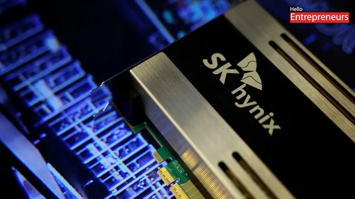








New Delhi: Demand for memory chips required for AI has been rising for South Korean chipmaker SK Hynix, which has begun construction on the new advanced chip packaging plant in Indiana, United States. The company’s groundbreaking took place Aug. 27 in West Lafayette, Ind.
The facility, at Purdue Research Park, will cost over $4 billion. It will be SK Hynix’s first major manufacturing site in the United States for the next generation High Bandwidth Memory (HBM) semiconductors, which have a significant role in AI systems and high-performance computing.
SK Hynix hopes to finish the build out of the cleanroom area by the second half of 2028 and will begin mass production of the next-generation HBM4E chips in the third quarter of 2029. The company is looking forward to processing hundreds of thousands of wafers annually from the plant.
The Indiana site will include an advanced HBM packaging line as well as a research and development centre for AI semiconductor technology. The SK Hynix will collaborate with Purdue University, customers and other partners to develop and test new packaging technologies.
The project also is anticipated to boost the U.S. semiconductor supply chain. The investment would create approximately 7,000 new jobs in the region, both directly and indirectly, says SK Hynix. The firm will also develop a more direct path for the U.S. business to the chip manufacturing sites in South Korea.
The transfer is happening as the AI boom spurs high demand for high performance memory. SK Hynix CEO Kwak Noh-Jung has said that the company does not expect the memory chip shortage to be resolved until 2030, therefore further production capacity is needed.
SK Hynix is now the largest producer of HBM in the world. The Indiana investment is part of a larger trend by chip makers to ramp up manufacturing and to move critical semiconductor activities to closer proximity to large US technology customers.