



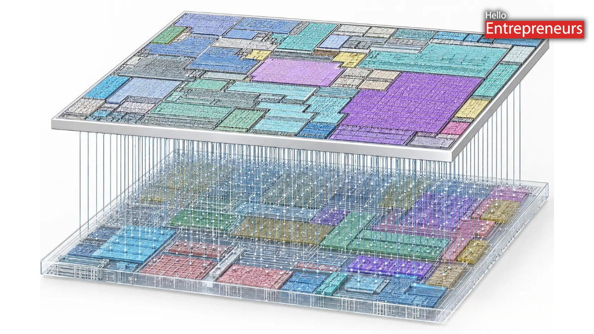
Huawei has unveiled its new smartphone SoC, Kirin 2026, featuring a technique it’s calling Logic Folding. According to the promotional materials, it’s a next-generation 3D stacked design that will transcend the physical constraints of traditional chip design.
Moving from flat to vertical
These days, most mobile processors are laid out in 2D, with the processing blocks nestled side by side on a flat plane. According to its graphic labels, Huawei calls this “limited by planar scaling.” It is increasingly difficult to include more performance in a given space as transistors get smaller.
The process of Logic Folding is different. The Kirin 2026 puts multiple layers of logic and memory into one place, rather than scattering them over one. The layers are connected by vertical interconnects which appear as gold-colored columns in the material. The logic layers are “folded” this way, reducing the distance the signals need to traverse and the energy that’s used moving data, Huawei states.
The headline numbers
All of the numbers in Huawei’s documents are “up to” numbers, which is the maximum performance:
- Up to 30% better performance
- Up to 40% better power efficiency
- Up to 1.5x transistor density
- Up to 50% more bandwidth
Lower latency and higher bandwidth are also cited as advantages of the stacked setup, the company also states. No test conditions, baseline chip or workloads have been revealed along with these figures, making it unclear what they are being compared to.
Density and power
Stacking is used to allow designers to put more transistors into a smaller area. Huawei estimates that this comes to about 1.5 times the transistor density, which is important for a phone chip because board space is limited. The denser the chip, the more processing units or memory resources that can be incorporated into it without increasing its size.
The other claim is power. The stacking and interconnect design is optimized for energy efficiency, and shorter vertical connections typically indicate lower energy consumption for transmitting data, according to Huawei. The real-world impact would be increased battery life or reduced heat during intensive use, like playing games or using the device’s artificial intelligence features.
The 50% bandwidth number refers to increased data transfer speeds between the logic and memory layers. It is a typical limitation on today’s mobile chips, particularly as AI capabilities require constant access to vast quantities of data.
Why it matters for Huawei
Since the export restrictions were imposed, the Kirin line has been one of the most important lines for Huawei. As transistors shrink more quickly than ever, sizes that are impractical or expensive to achieve, architectural techniques such as 3D stacking can be used to enhance performance beyond just smaller process nodes. Huawei’s tagline for the chip is “Beyond Limits”, which suggests that.
At the bottom of its graphic, the company abstracts the design into five phrases – 3D Stacked, Logic Folding, More Power, Less Power and Beyond Limits. More Power, Less Power” is a pairing of higher performance and less power consumption.
What is still unknown
There are some facts that are not mentioned in the material that are important. No details of the manufacturing process node, CPU and GPU configuration, clock speeds or which phones will get the chip are included. Huawei has not given a launch date or a list of devices. The real world performance will need independent benchmarks to check whether it approaches the “up to” performance.
However, stacked chip designs introduce engineering challenges as well, such as heat dissipation between layers, and manufacturing yield, as a defect in one chip can impact the entire stack. Huawei’s material doesn’t state how it addresses these problems.
The Kirin 2026, for the time being, is a set of claims and a design concept. Of course, the significance of Logic Folding in actual mobile phones will rely on the kit which is set to be issued and its performance outside of the lab.